
New theme at LINXS aims to combine semiconductor device development with advanced characterisation through X-rays and neutrons
Semiconductors power almost all electronics and can enable breakthroughs in clean energy, electric vehicles and the use of AI. A new theme at LINXS, X-ray and neutron-based characterisation of advanced semiconductors (Semiconductors), aims to combine semiconductor device development with advanced characterisation using X-rays and neutrons.
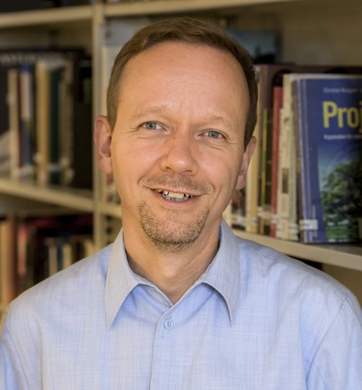
Semiconductor technology is now at a pivotal point where X-rays and neutrons can play a big part in advancing development according to Rainer Timm.
– It is an exciting time to do research in this field. For decades it was silicon, silicon, nothing but silicon which was used in the semiconductor industry, but now there is an increasing need for completely new concepts. Materials are for example used in mobile phones that for a long time were only found in academic research labs, says theme leader Rainer Timm, Professor at the Department of Physics, Lund University.
He was motivated to start the theme as the technology is now at a pivotal point. The rise of AI has necessitated new types of semiconductor devices and materials, as conventional silicon-based transistors are not optimised for regenerative AI, which is run on increasingly powerful computers. Training AI models also requires enormous amounts of energy: comparable to the energy needs of a smaller city.
Electrification is another societal change accelerating the need for novel semiconductor technologies. Currently, much energy is wasted due to insufficient or ineffective energy conversion. As more sectors transition to renewable energy to move away from fossil fuels, this problem becomes even more critical to solve, as solar and wind energy sources require fast power electronics and efficient storage systems.
X-rays and neutrons can accelerate new semiconductor device development
Deepened fundamental understanding of how materials behave can solve many of these challenges, according to Rainer Timm. X-ray and neutron techniques are especially suited for the characterisation of new semiconductor materials as they can reveal fundamental processes down to the nanometre scale. This means that they have potential to half the energy usage of AI models, for example, and to convert power more efficiently and at higher frequency.
– We are now in a position to study different semiconductor materials at the atomic scale, including interfaces and ultrathin layers as they are used in industry.
– With X-rays, we can also study the complex environment around the semiconductor channel itself, and analyse the interplay between the semiconductor and its surrounding materials: for example, what happens when you replace the insulator material around the semiconductor, or when you apply voltage pulses or a constant electric field?
X-rays and neutrons also allow for the study of complex devices during processing or during electrical operation, as one, for example, implements a processing step into a synchrotron beamline.
– We have noticed that the chemical reaction that occurs when you operate a device is more complex than what we previously thought. Understanding what happens during this process will be key to improve power conversion or energy storage, says Rainer Timm.
Strengthen interaction and collaboration different groups of experts
Yet, up now, the use of X-rays and neutrons have been low within the semiconductor community, partly due to lack of knowledge on how to use the techniques. Thus, the theme aims to strengthen interaction and collaboration between experts in material characterisation and semiconductor device development, both from academia and industry, in Sweden and in Europe. Through activities such as conferences, workshops and seminars, the theme will bring different people together.
Being at LINXS will further support this mission emphasises Rainer Timm.
– With LINXS being so close to the MAX IV and ESS facilities, it will be easier to attract external collaborators. It will also enable us to do things on a multilateral level. The whole aim is to create something new, that is more than just a bilateral connection which is the case for many other research projects.
The theme starts in January 2026 and will organise its work in four working groups: WG 1: Advanced Transistor Technology; WG 2: Power Electronics; WG 3: Neuromorphic Materials for Deep Learning and AI; and WG 4: Optoelectronics and Photovoltaics.
At the end of the theme, Rainer Timm hopes they have succeeded in building a critical mass of people who can continue to progress basic material research with the help of X-rays and neutrons. He would also like to see new methodologies for characterising novel materials.
– It will be important to sustain the network after the theme ends, with the ultimate goal to develop fundamental understanding of how to create hitherto new semiconductors.